Technology
Applied Materials goes to 20% of Besi as chip packaging becomes the prize
Applied Materials is more than doubling its holding in the Dutch hybrid-bonding specialist. The move says the next bottleneck in AI hardware sits in how chips are stacked, not only in how they are printed.
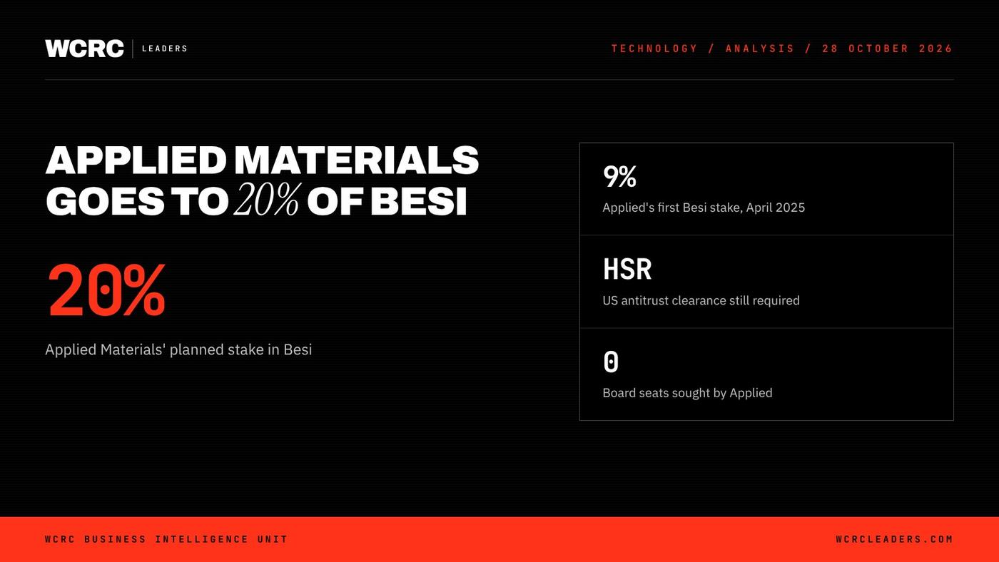
At a glance: WCRC Leaders' assessment: Applied's move to about 20% of Besi is a bet that hybrid bonding becomes the gatekeeper of AI memory and logic, and countries building packaging plants now must plan for it. On 26 October 2026, Applied Materials said it will raise its Besi stake to about 20% through an accelerated share purchase, subject to US antitrust clearance. It first bought in during April 2025. It seeks no board seat and no larger stake. Besi's orders nearly doubled year on year in the third quarter.
What exactly has Applied Materials agreed?
Applied Materials announced on 26 October 2026 that it will raise its strategic investment in BE Semiconductor Industries (Besi), the Amsterdam-listed maker of chip assembly equipment, to approximately 20% of Besi's outstanding shares. It has entered an accelerated share purchase agreement; delivery is subject to the expiry or termination of the waiting period under the US Hart-Scott-Rodino Antitrust Improvements Act.
The purchase adds to the holding Applied first built in April 2025, when Besi stated that Applied had bought nine percent of its shares in market transactions.
Applied set clear limits: no current intention of going beyond about 20%, no board seat, and a long-term horizon. Neither company disclosed a price or deal value.
Dr Prabu Raja, President of Applied's Semiconductor Products Group, gave the rationale: "Applied Materials is adding to its investment in Besi as hybrid bonding technology and next-generation interconnect architectures become increasingly critical enablers of energy-efficient AI compute performance." He added: "We also look forward to furthering our strategic collaboration with Besi and delivering the innovative products and technologies our customers need to scale AI systems."
Besi acknowledged the announcement on 27 October from Duiven in the Netherlands. Chief executive Richard Blickman said Besi welcomed the larger stake as "further confirmation of Besi's hybrid bonding and wafer-level assembly strategy".
Why does hybrid bonding matter so much?
For decades, chip progress came mainly from shrinking transistors. AI accelerators now depend as much on stacking and joining chips, from memory dies piled into high-bandwidth memory (HBM) to stacked logic. Hybrid bonding joins copper directly to copper, with no solder bumps or underfill, giving tighter connections and better heat control.
The two companies have worked together since 2020, and Besi recently joined Applied's EPIC Center as an Innovation Partner. Joint work covers 3D IC scaling, logic and memory integration, thermo-compression bonding, and die-on-wafer, die-on-die and die-on-panel platforms.
The memory makers explain why the timing matters. A technical note published on SK hynix's newsroom in August 2026 says package height rises from 720 micrometres to 775 micrometres from HBM4, that limits on existing methods are likely to emerge from HBM4E onward, and that full-scale hybrid bonding adoption in HBM is "most likely" at HBM4E or HBM5. It adds that the timing "remains uncertain". Samsung said in March 2026 that its hybrid copper bonding "will enable next-generation HBM to achieve 16 or more layers". TSMC's SoIC 3D stacking technology uses a bond pitch that "starts from the sub-10µm rule" and can be integrated into its CoWoS and InFO packaging.
Is the demand real or a story?
Besi's own numbers point to real orders. For the third quarter of 2026, it reported revenue of €283.4m, up 113.6% year on year, and orders of €342.6m, up 96.1%. Net income rose 323.7% to €107.2m and gross margin was 65.2%. Besi said hybrid bonding orders in the first nine months of 2026 more than doubled against the whole of 2025, and cumulative demand now exceeds 215 systems.
There is a caution. Besi guided fourth-quarter revenue flat to plus or minus 5%, as some customers asked for deliveries to match their production plans for the first half of 2027. Timing is set by a few very large buyers.
Analysis: For Applied, a 20% holding without a board seat is a way to stay close to a critical tool supplier, share engineering roadmaps and avoid the regulatory weight of a full takeover. For rival bonding-tool makers, it raises the bar.
What does it mean for India's packaging push?
India has chosen assembly, test and packaging as its fastest route into chips. The India Semiconductor Mission had approved 10 projects worth ₹1.60 lakh crore across six states by December 2025, and the first plants to produce are packaging units.
Micron India, a WCRC MegaBrand in semiconductor design and fabrication, opened its Sanand assembly and test plant on 28 February 2026, backed by about $2.75bn from Micron and government partners. It expects to handle tens of millions of memory chips in 2026, rising to hundreds of millions in 2027. CG Semi, the venture led by CG Power and Industrial Solutions, one of WCRC 1000, India's Most Valuable Enterprises 2026, with Renesas and Stars Microelectronics, began commercial packaging at Sanand on 4 July 2026. The government noted production launches at Kaynes Technology, one of WCRC 1000, India's Most Valuable Enterprises 2026, in the same region.
Tata Electronics is investing $3bn in its packaging plant at Jagiroad, Assam, approved in 2024 for flip chip and integrated system-in-package technologies. On 17 September 2026, it signed an agreement with Besi to use Besi's advanced packaging equipment and technologies at Jagiroad. Tata Electronics chief executive Dr Randhir Thakur said then that "advanced packaging is rapidly becoming one of the most critical differentiators in semiconductor innovation."
Analysis: Assam was approved for flip chip and system-in-package work, a sound starting point. But the highest-value AI work is moving to hybrid bonding and 3D stacking, where tools are scarce and know-how sits with a few firms. The Tata and Besi link gives India a door into that tool chain, and device makers such as Dixon Technologies, one of WCRC 1000, India's Most Valuable Enterprises 2026, stand to gain from deeper local component supply.
Who gains and who is exposed in Asia and the Gulf?
In Korea, SK hynix and Samsung, a WCRC MegaBrand in televisions, are racing to stack 16 or more memory layers. SK hynix shipped 12-layer HBM4E samples in June 2026 using its advanced MR-MUF process, and Samsung shipped 12-layer HBM4E samples in May. Taiwan's TSMC already integrates 3D-stacked chips into its CoWoS packaging. Analysis: the first memory maker to reach good hybrid bonding yields at 16 layers is likely to gain in the next round of AI memory contracts. Samsung also appears among the World Brands in India's Most Powerful Brands 2026 by WCRC.
Analysis: For Gulf states building AI capacity, the lesson is about where control sits. National champions such as G42 have focused on data centres and compute. Packaging know-how, the layer Applied is now consolidating, remains with a handful of US, European and East Asian firms. Gulf investors that want more than a buyer's seat will need partnerships in packaging and test.
The WCRC View
The WCRC Business Intelligence Unit reads this as a clear signal: the contest in AI hardware has widened from lithography and transistors to the way chips are joined. Applied's choice of a large minority stake, rather than a bid, shows how sensitive this layer has become to regulators and customers alike.
Who gains: Besi, which gains a long-term anchor shareholder while keeping its independence; Applied, which deepens its access to a key bonding roadmap; and memory makers that can move to hybrid bonding early. Who is exposed: rival tool makers without a partner of similar scale, and packaging plants built only for older methods.
What leaders should do now: boards in India's electronics and semiconductor value chain should ask management whether plant plans include a credible path to advanced 3D and hybrid packaging, and which equipment partners would deliver it. Gulf investors should test whether their AI strategies own any part of packaging and test, or only buy finished capacity.
What WCRC will watch next: clearance of the US antitrust waiting period and the delivery of the shares; Besi's fourth-quarter results and its 2027 hybrid bonding order book; which memory maker confirms hybrid bonding in volume HBM; and whether the Tata and Besi partnership at Jagiroad moves from training to installed advanced packaging tools.
Further reading: SK hynix shelves the Solidigm IPO: what it says about the AI capex cycle, TSMC and ASML post records, and ASML says supply falls short to 2028 and UAE pledges €15bn more for Greece as G42 eyes an AI factory.
Quick answers
Q: How big will Applied Materials' stake in Besi be? A: About 20% of Besi's outstanding shares, up from the nine percent Besi said Applied bought in April 2025.
Q: Does the deal need approval? A: Yes. Delivery of the shares depends on the expiry or termination of the US Hart-Scott-Rodino antitrust waiting period.
Q: Will Applied take a seat on Besi's board? A: No. Applied said it does not intend to seek board representation and has no current intention to go beyond about 20%.
Q: What is the link to India? A: Tata Electronics signed an agreement with Besi in September 2026 to use Besi's advanced packaging equipment at its $3bn plant in Jagiroad, Assam.
SK hynix shelves the Solidigm IPO: what it says about the AI capex cycle
Junior hires fall to 9% at Anthropic: a warning for India's IT pyramid

Supplier-funded compute: what CFOs should read into the AI financing loop
Google Cloud doubles revenue as Alphabet funds AI with debt
China's 40-technology export list puts India's solar push on notice
TSMC and ASML post records, and ASML says supply falls short to 2028
Filed under